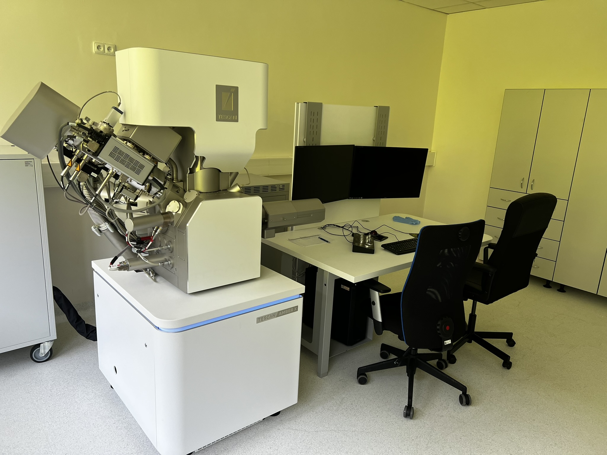
The SEM-FIB laboratory is equipped with a high-resolution scanning electron microscope TESCAN AMBER X, combined with a plasma focused ion beam (Xe Plasma FIB). This cutting-edge system enables advanced microstructural analysis of a wide range of materials and serves as a tool for research, teaching and training across materials-oriented disciplines.
The microscope is equipped with a high-brightness Schottky emission cathode, which enables imaging with a resolution of up to 0.9 nm at an acceleration voltage of 15 keV, 1.5 nm at 1 keV and 0.8 nm in STEM mode. Thanks to the beam deceleration mode, a resolution of up to 1.3 nm is achieved even at low voltages. The acceleration voltage range ranges from 50 eV to 30 keV and the beam current can be set in the range from 2 pA to 400 nA. The microscope is also capable of operating in low vacuum mode up to 500 Pa, which allows the analysis of non-conductive or sensitive samples without the need for a conductive coating. The device includes a unique rocking stage, i.e. a tilting sample holder, which significantly facilitates the acquisition of high-quality data for 3D FIB-SEM tomography and reduces the formation of artifacts during the reconstruction of volumetric structures.
The detection system includes a wide range of detectors: a secondary electron detector with an extraction lens (Everhart-Thornley SE) and a backscattered electron detector (LBSE), as well as in-lens SE and BSE detectors for high-contrast imaging with high resolution, as well as analytical detectors EDS and EBSD from Oxford Instruments, which are used for chemical analysis of elemental composition, phase identification and crystallographic characterization. The instrument is also equipped with a nano-manipulator, which allows for the preparation of slides, precise manipulation and microoperations directly in the chamber. The microscope contains one GIS system (Pt).
TESCAN AMBER X is a key tool for detailed characterization of metals, ceramics, composite materials, layers, porous structures and degraded materials. It is designed for the analysis of microstructure, chemical composition, crystallography and mechanical properties at the nanometric scale.

